使用Vivado进行FPGA设计流程简介
本文使用软件版本:
Vivado 2017.4
ModelSim SE-64 10.5
1. FPGA设计流程

与ASIC设计流程相似,FPGA开发也包括RTL级代码编写、功能验证(前仿真)、逻辑综合、形式验证、后端布线以及STA等步骤。其中逻辑综合、后端布线以及下载到FPGA芯片中使用Vivado。各级仿真步骤可使用Vivado自带仿真工具,也可用第三方软件Modelsim(windows平台)或VCS(Linux平台)等。
2. 建立工程
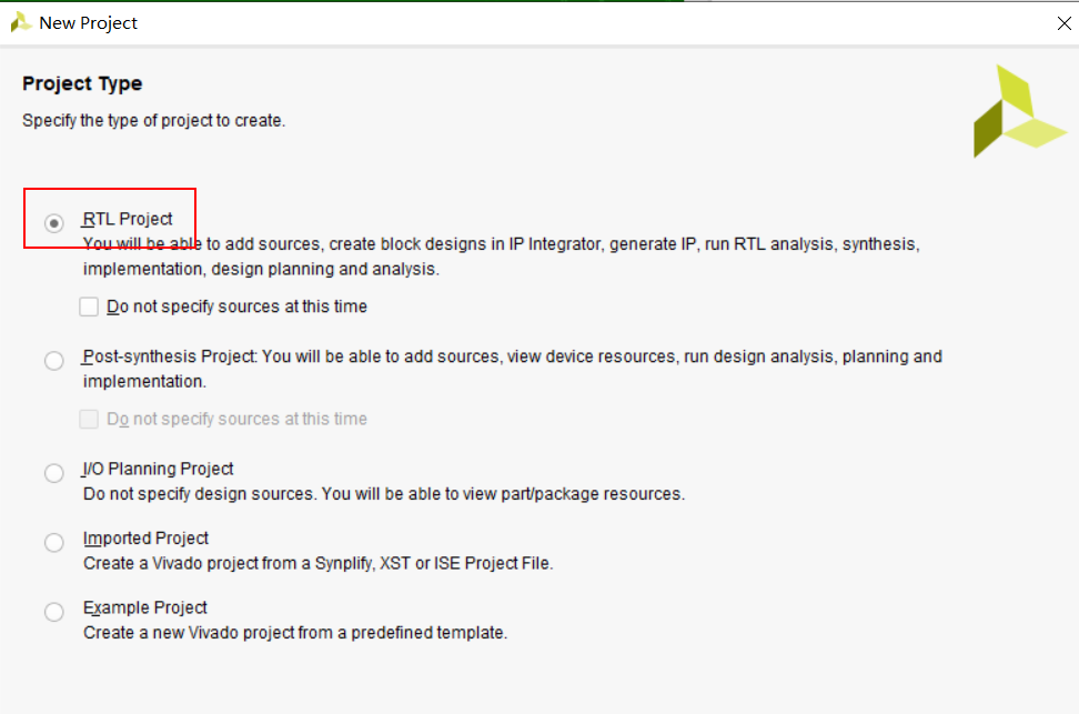
a、使用Vivado来建立工程,而不是Vivado HLS。(Vivado使用直接编写HDL代码;Vivado HLS则编写C/C++代码并转化为硬件描述语言)。工程建立时选择RTL Project。
b、在工程中设置第一个HDL的source文件,此时可以选择Verilog、System-Verilog或VHDL等文件类型。

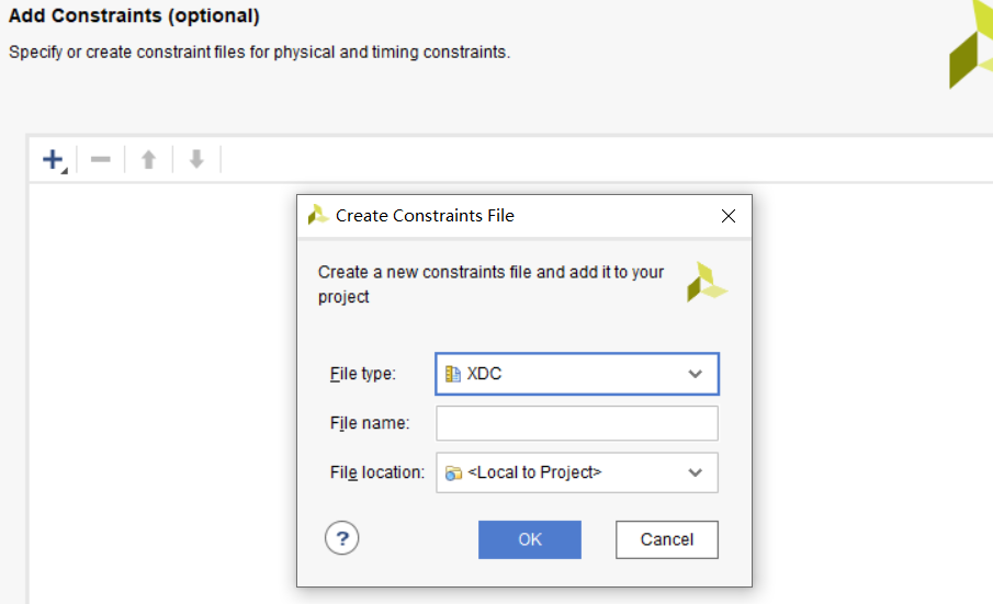
c、约束文件只支持XDC文件类型。具体的XDC编写规范参照官方文档。
UG625:https://china.xilinx.com/support/documentation/sw_manuals/xilinx14_7/cgd.pdf UG903:https://www.xilinx.com/support/documentation/sw_manuals/xilinx2017_4/ug903-vivado-using-constraints.pdf
我们需要编写规范的代码,能做多好就做多好,这样可以尽可能降低编译器的工作难度,如果再适时地给编译器一些恰当的指导和建议(通过约束),就可以使FPGA设计更加高效。
d、芯片型号选择使用的对应芯片即可。
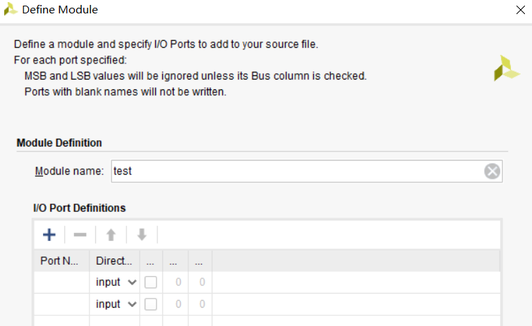
e、建立工程后会提示输入第一个module的名称,建议与source文件名称相同。
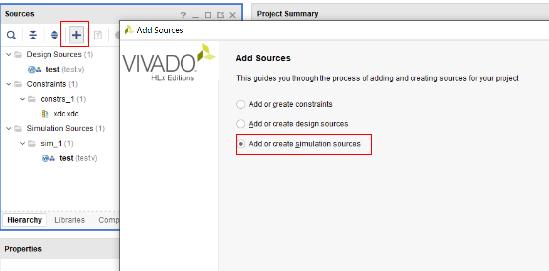
f、通过add sources来添加testbench。
至此,工程建立完毕,在test和test_bench中编辑好代码后就可以进行仿真以及比特流下载了。
3、仿真分析
本文使用了一个的分频器作为测试例程。test.v及test_bench.v文件内容见附录1及附录2。
a、RTL分析
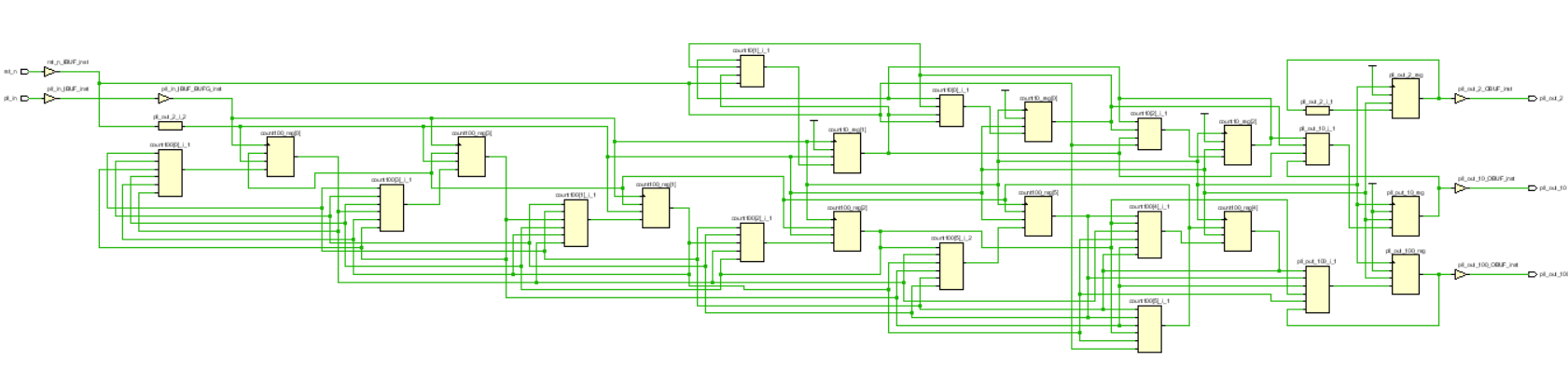
点击RTL analysis—Open Elaborated Design—Schematic可以得到RTL代码反映出来的电路结构。
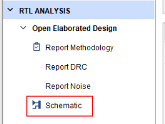
可以通过实时对比电路和代码,找到代码设计的缺陷。

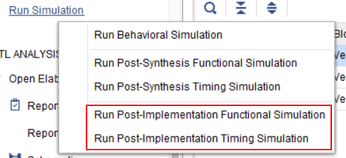
b、前仿真
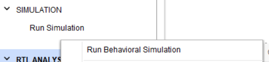
在Simulation中的Behavioral Simulation中可以对电路的功能进行仿真。(此处使用vivado自带的仿真工具)
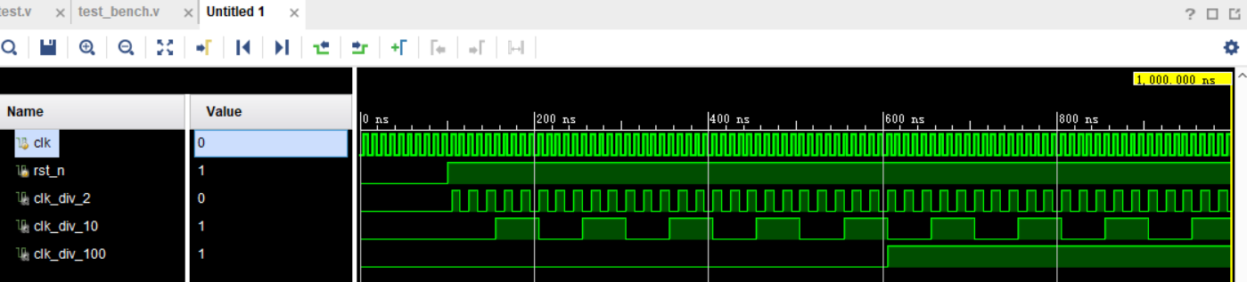
可以在scope中观察各信号的波形。
c、综合
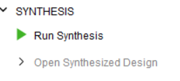

点击Synthesis对RTL代码进行综合,综合完成后需要对综合后的代码进行IO设置和约束。
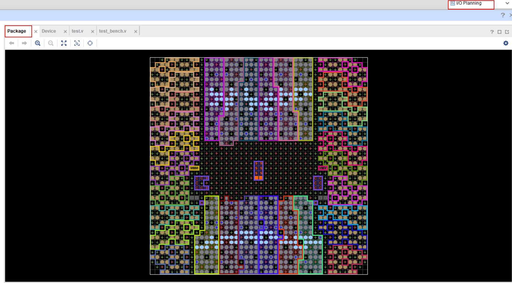
在点击Open Synthesized Design后弹出package代表了实际芯片的引脚图。在I/Oports中选择合适的输入输出引脚。(如果不选择输入输出引脚,下载到芯片中会无功能)

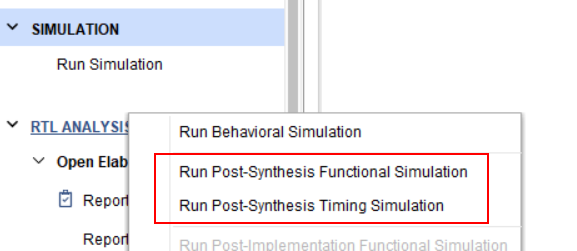
此时可以点击综合中的原理图以及仿真中的post-synthesis simulation对综合后的net网表进行电路分析以及形式验证、时许分析等。
d、布局实现
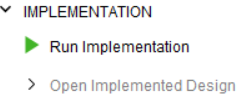
在设置了IOports、完成了形式验证以及STA之后,点击run Implementation进行电路实现。实现后也可同过仿真进行STA验证以及后端验证。
e、生成二进制文件,下载
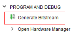
生成二进制文件,通过jtag下载到芯片。手中暂无fpga,不演示。
第三方仿真器与Vivado联合仿真
由于Vivado自带仿真器功能较少,通常使用ModelSim等第三方仿真器进行联合仿真,网上教程较多,不赘述。
附录1:test.v
1
2
3
4
5
6
7
8
9
10
11
12
13
14
15
16
17
18
19
20
21
22
23
24
25
26
27
28
29
30
31
32
33
34
35
36
37
38
39
40
41
42
43
44
45
46
47
48
49
50

module test(pll_in,rst_n,pll_out_2,pll_out_10,pll_out_100);
input pll_in;
input rst_n;
output reg pll_out_2;
output reg pll_out_10;
output reg pll_out_100;

reg [3:0] count10;
reg [6:0] count100;
//二分频
always @(posedge pll_in or negedge rst_n) begin
	if (!rst_n) begin
		pll_out_2<=1'd0;
	end
	else pll_out_2<=~pll_out_2;

end
//十分频
always @(posedge pll_in or negedge rst_n) begin
	if (!rst_n) begin
		pll_out_10<=1'd0;
		count10<=4'd0;
	end
	else if (count10<4'd5) begin
		pll_out_10<=pll_out_10;
        count10=count10+1;
    end
    else begin
        count10<=4'd1;
        pll_out_10<=~pll_out_10;
    end
end
//100分频
always @(posedge pll_in or negedge rst_n) begin
    if (!rst_n) begin
        pll_out_100<=1'd0;
        count100<=7'd0;
    end
    else if (count100<7'd50) begin
        pll_out_100<=pll_out_100;
        count100=count100+1;
    end
    else begin
        count100<=7'd1;
        pll_out_100<=~pll_out_100;
    end
end
endmodule
附录2:test_bench.v
1
2
3
4
5
6
7
8
9
10
11
12
13
14
15
16
17
18
19
20
21
22
23
24
25
26

module test_bench();
reg clk;
reg rst_n;
wire clk_div_2;
wire clk_div_10;
wire clk_div_100;

test dut (.pll_in(clk),.rst_n(rst_n),.pll_out_2(clk_div_2),.pll_out_10(clk_div_10),.pll_out_100(clk_div_100));

initial begin
	clk=1'd0;
	rst_n=1'd0;
	#100
	rst_n=1'd1;
	#1000
	$finish;
end
//输入时钟100MHz
always 	#5 clk=~clk;
//下面的代码仅用于verdi调试使用
//initial begin
//	$fsdbDumpfile("test_plus.fsdb");
//	$fsdbDumpvars();
//end
endmodule